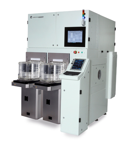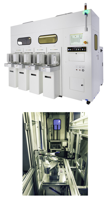

YES-VertaCoat (automated)

The YES-VertaCoat automated, silane vapor deposition system is designed for today’s most advanced MEMS and semiconductor process applications. Whether it’s precise surface modification to reduce stiction for MEMS devices or a thin copper diffusion barrier layer in an advanced semiconductor device, the capability to use a large number of different organosilanes provides the ability for precise surface modification. Flexibility of production is assured with an optional chemical delivery system that can handle up to 5 different chemicals in a precise controlled operation.
The YES-VertaCoat Silane Vapor System is designed for high-volume production, using an EFEM with one or two load ports and a wafer handling robot inside an integrated Class 1 minienvironment. The system incorporates the laminar flow technology of the YES-PB series. The laminar flow for the process chamber and the clean work cell environment provide the particle control required for nanoscale wafer processing.
Up to 50 wafers are loaded into a stainless steel cassette-type rack on the oven chamber door and, when loading is complete, lifted up into the process chamber. A staging area enhances throughput by preloading wafers onto a cassette while production wafers are being processed in the chamber. The cassette-type rack can be designed specifically for either 200mm or 300mm wafers. An optional versatile wafer cassette module (25 wafers capacity) is designed to accommodate both 200mm and 300mm wafers for flexible MEMS production.
MEMS Applications
- Wafer dehydration
- The moisture on the surface of wafers will cause unintended reactions with various deposition steps. These reactions result in unstable surface which degrade over time. Vacuum dehydration provides a clean stable starting surface resulting in superior films.
- Surface Tension Modification
- As devices are made smaller and smaller, static friction (stiction) becomes more and more significant. By modifying the surface tension with a class of fluorinated organosilanes, the operating life of moving parts in MEMS devices can be significantly lengthened. Conversely, if surfaces need to be bonded together, other organosilanes can be coated which enhance bonding strengths between unlike materials.
Semiconductor Process Applications
- Copper diffusion barrier
- For nanoscale devices, the thickness of conventional metal barrier layers between copper and the low-k dielectric cannot be reduced sufficiently without affecting barrier effectiveness. Self-assembling monolayers of a variety of organosilanes provide a thin and effective diffusion barrier, resulting in reduced copper line resistance.
- Copper to low-k adhesion layer
- Aminosilanes and mercaptosilanes provide specific bonding sites for copper. The surface can be precisely modified to optimize adhesion and to minimize copper voids during copper deposition.
- Porous dielectric repair
- Vapor deposition can restore low-k dielectrics that are plasma (ash) damaged. More information on low-k dielectrics here.
Benefits
As technology shrinks, there is a growing need for precise control over nanoscale surface areas. Silane vapor deposition is a process that assists in the deposition of monolayer films of various chemistries in order to achieve precise surface modification. Compared to wet chemistry, vapor deposition is the preferred method for coating surfaces with organosilanes, as trapped wet chemicals in high-aspect ratio features, as an example, corrode copper. YES vapor deposition systems provide total environmental control over the deposition process and accommodate a variety of functionally diverse silanes, for a variety of processes, on a variety of surfaces.
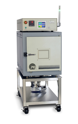
YES-VertaCoat is designed to achieve tight control over your process conditions:
- Controlled temperature ramp up and cool down (up to 200ºC)
- Controlled hydrolysis process due to a dry inert ambient
- Precise amount of liquid is vaporized for consistent deposition
- Horizontal laminar flow for increased particle isolation and removal (for most processes, average particle addition is calculated to be < 0)
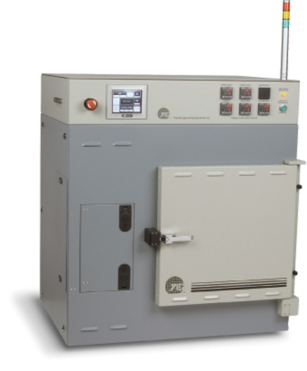
Reproducible process results with process step control for:
- Speed of liquid
- Vaporization chamber temperature
- Vapor line temperature
- Process vacuum chamber temperature
- Process starting pressure
- Process time for vapor deposition